


Solder bridging, also known as the formation of solder resistance bridges, is one of the most common challenges in precision welding and PCB assembly. It occurs when excess solder unintentionally connects two or more conductive areas, leading to electrical shorts, component failure, or performance instability. Understanding the causes and prevention of solder resistance bridges is essential to maintaining high reliability in modern electronic manufacturing.
What Are Solder Resistance Bridges?
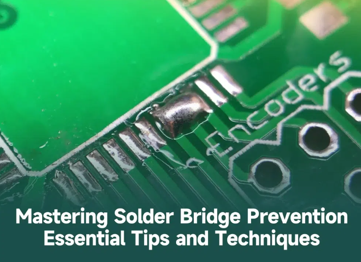
Solder resistance bridges refer to unintended solder connections between conductive traces or pads. These bridges typically form during the reflow or manual soldering process when molten solder flows beyond the intended area. In printed circuit boards (PCBs), solder resistance bridges disrupt circuit function and can cause catastrophic short circuits.
In advanced semiconductor packaging and precision welding, solder resistance bridges compromise hermeticity, reliability, and long-term stability. The purpose of controlling these bridges is not only to avoid immediate defects but also to ensure that solder joints maintain their integrity over thousands of operational cycles.
Why Do Solder Resistance Bridges Form?
There are multiple reasons behind the formation of solder resistance bridges, most of which stem from design, material, or process errors. The most common causes include:
- Excess Solder Application: Applying too much solder paste or using an incorrect stencil thickness during printing can lead to overflowing solder that connects nearby pads.
- Inadequate Pad Spacing: Pads or traces placed too close together increase the risk of bridging, especially in fine-pitch components.
- Uneven Heating During Reflow: Inconsistent temperature distribution may cause uneven solder flow, promoting bridge formation.
- Contaminated Surfaces: Dirt, oxidation, or residual flux can alter surface tension, leading to unwanted solder accumulation.
- Improper Wetting: When solder fails to wet properly, it tends to migrate unevenly, forming solder resistance bridges between adjacent areas.
Each of these issues reflects the delicate balance between thermal control, surface preparation, and precision in solder application.
How Does PCB Design Influence Solder Resistance Bridges?
The layout of a printed circuit board plays a critical role in preventing solder resistance bridges. Proper design ensures that solder has sufficient room to flow and solidify without forming unwanted connections.
Designers should:
- Maintain adequate spacing between pads based on IPC standards.
- Incorporate solder mask dams (narrow strips of solder mask between pads) to prevent solder migration.
- Use optimized pad geometry to control solder volume and flow direction.
- Ensure uniform trace widths to maintain consistent heat distribution.
In modern manufacturing, computer-aided design tools are often used to simulate solder flow and detect potential bridging risks before production begins.
What Role Does Solder Paste Quality Play in Bridging?
The composition and quality of solder paste have a direct impact on the likelihood of forming solder resistance bridges. Key factors include:
- Viscosity: Low-viscosity pastes tend to spread excessively, increasing the risk of bridging.
- Particle Size: Fine solder particles promote even melting but can also flow into unintended areas if not properly controlled.
- Flux Content: The type and amount of flux affect solder wetting and flow behavior. Too much flux may cause spattering or bridging.
- Storage Conditions: Improper storage can degrade solder paste consistency, making it more prone to defects.
To minimize issues, manufacturers often implement strict quality control for solder paste preparation and handling.
How Can the Reflow Process Be Optimized to Prevent Bridges?
Reflow soldering is one of the most critical stages in preventing solder resistance bridges. An optimized temperature profile ensures uniform melting and solidification. Key considerations include:
- Preheat Zone: Gradually warms the board to activate flux and remove moisture, preventing solder splatter.
- Soak Zone: Ensures temperature uniformity across all components, minimizing uneven solder flow.
- Reflow Zone: Must reach the ideal peak temperature for full wetting without overheating the solder paste.
- Cooling Zone: Controls the solidification rate to avoid movement and bridging.
Advanced equipment, such as the vacuum reflow ovens developed by Chengliankaida Technology Co., LTD, provide precise control of temperature and atmosphere, effectively reducing solder resistance bridges and void formation.
How Does Vacuum Soldering Reduce Solder Resistance Bridges?
Vacuum soldering technology offers a highly controlled environment for advanced packaging and power semiconductor assembly. By removing trapped air and contaminants during the reflow process, it significantly lowers the probability of solder resistance bridges.
Benefits of vacuum soldering include:
- Elimination of Air Pockets: Reduces voids that can alter solder flow patterns.
- Enhanced Wetting Behavior: Improves solder adhesion and uniformity across surfaces.
- Stable Thermal Profile: Ensures consistent melting and cooling for fine-pitch components.
- Higher Reliability: Results in stronger, more consistent joints with lower failure rates.
Precision vacuum soldering equipment, such as systems from Chengliankaida Technology Co., LTD, demonstrates superior performance in reducing both solder resistance bridges and overall void rates in hermetic packages.
What Process Control Methods Help Prevent Solder Resistance Bridges?
Modern electronics manufacturing employs advanced process control to detect and prevent solder resistance bridges. Key methods include:
- Automatic Optical Inspection (AOI): Detects bridging and alignment issues early in the production line.
- Solder Paste Inspection (SPI): Ensures correct solder volume and placement before reflow.
- Temperature Profiling: Monitors thermal uniformity to optimize the reflow process.
- Statistical Process Control (SPC): Tracks process data to identify deviations leading to bridging.
Integrating these control systems helps maintain consistent soldering quality and reduce rework or scrap rates.
What Are the Best Practices to Minimize Solder Resistance Bridges?
To achieve reliable soldering without bridges, manufacturers should adopt the following best practices:
- Design for Manufacturability (DFM): Review PCB layouts for spacing and mask optimization.
- Maintain Clean Surfaces: Ensure pads are free from oxidation and contamination.
- Use Accurate Stencils: Select proper stencil thickness and aperture shape to control solder volume.
- Control Process Parameters: Calibrate printing pressure, alignment, and reflow profiles regularly.
- Perform Continuous Inspection: Apply AOI and X-ray systems to monitor and verify solder joint quality.
These practices ensure that solder resistance bridges are minimized, improving both electrical performance and product longevity.
What Are Future Trends in Preventing Solder Resistance Bridges?
With the advancement of miniaturized and high-density electronic packaging, the challenge of solder resistance bridges is becoming more complex. Future developments will focus on:
- AI-Based Defect Prediction: Using machine learning to anticipate and correct bridging tendencies in real time.
- Nanotechnology Solder Materials: Formulations that provide better flow control and lower surface tension.
- Automation and Robotics: Ensuring precision in solder paste printing and component placement.
- Improved Vacuum Systems: Offering cleaner, more stable environments for defect-free soldering.
As technology evolves, the prevention of solder resistance bridges will rely on both smarter design and more sophisticated process control.
Conclusion
Solder resistance bridges represent a significant reliability concern in modern precision welding and semiconductor packaging. Their prevention requires careful attention to PCB design, solder paste characteristics, temperature control, and real-time inspection.
By understanding the mechanisms behind solder resistance bridges and applying optimized vacuum soldering techniques, manufacturers can significantly improve product yield and performance stability. As the industry moves toward higher integration and miniaturization, advanced process control and intelligent automation will remain central to eliminating solder bridging and ensuring long-term reliability.
Comments