


Introduction:
The semiconductor industry has long been one of the driving forces of technological innovation, and at its heart lies wafer fabrication — a complex process that requires precision, cleanliness, and efficiency. Over the past few decades, the evolution of wafer handling systems has significantly impacted the productivity and quality of semiconductor production. Among the leaders in this revolution are Kawasaki Robotics and Daihen Corporation, two pioneering companies that are reshaping the standards of wafer handling robotics and driving improvements in cleanroom environments.
Both Kawasaki and Daihen have developed cutting-edge solutions that are addressing the growing demands of semiconductor manufacturing, offering automation, precision, and enhanced safety. With the ever-increasing complexity of integrated circuits and the demand for faster, more efficient production, these companies are playing a crucial role in advancing the future of wafer handling and cleanroom standards.
The Growing Need for Wafer Handling Robotics in Semiconductor Manufacturing
The semiconductor manufacturing process involves the intricate handling of silicon wafers, which are thin slices of semiconductor material used to create integrated circuits. These wafers are subjected to a series of high-precision steps, including photolithography, etching, deposition, and testing. Each stage of this process requires carefully controlled handling to avoid contamination, damage, or loss of accuracy.
Semiconductor cleanrooms are tightly regulated environments designed to minimize the presence of airborne particles, ensuring that even the smallest particle of dust or debris does not interfere with the delicate work being done on wafers. As technology advances, wafer handling becomes increasingly complicated, requiring more specialized equipment to ensure precision while maintaining the stringent cleanliness required by the semiconductor industry.
Here, wafer handling robotics come into play. These robots are designed to automate the handling, movement, and inspection of wafers in a cleanroom setting, helping improve production speed, accuracy, and cleanliness. By using advanced robotics, semiconductor manufacturers can enhance overall operational efficiency, reduce human error, and ensure that each wafer remains uncontaminated throughout the process.
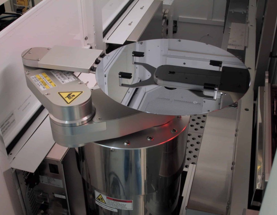
Kawasaki Robotics: Leading the Way in Wafer Handling Innovation
Kawasaki Robotics, a key player in the industrial automation field, has long been recognized for its contributions to robotics in various industries, including semiconductor manufacturing. The company has developed a series of wafer handling robots designed to meet the increasingly stringent requirements of the semiconductor industry.
Kawasaki's dual-arm robots, such as the RS003N, are a prime example of innovation in wafer handling. These robots are engineered to work with high precision and speed, handling wafers with remarkable delicacy and ensuring that contamination risks are minimized. Designed to operate within the tightly controlled conditions of cleanrooms, Kawasaki’s robots feature specialized sealed structures and cleanroom-compliant materials that prevent particles from escaping into the environment.
Key Features of Kawasaki's Wafer Handling Robotics:
High Precision and Speed: Kawasaki's robots are designed to perform tasks with utmost precision, moving wafers quickly and efficiently through the manufacturing process. This improves productivity while maintaining the integrity of the wafers.
Advanced Motion Control: Kawasaki's robots use advanced motion control technology to ensure that movements are smooth and calculated, preventing unnecessary shocks or vibrations that could affect the wafer handling process.
Cleanroom Compatibility: Kawasaki's robots are specifically designed to meet the cleanliness standards of semiconductor cleanrooms, with features such as low particle generation, easy-to-clean surfaces, and compatibility with ISO Class 1 environments.
Flexibility in Wafer Handling: These robots are capable of handling various wafer sizes and are adaptable to different wafer-processing machines, which is crucial in meeting the diverse needs of semiconductor manufacturers.
Kawasaki’s continued innovation in wafer handling robotics is helping to optimize production processes, reduce downtime, and elevate cleanroom standards in semiconductor manufacturing. The integration of Kawasaki robots into wafer fabrication facilities has significantly improved workflow efficiency, making them a key player in advancing semiconductor technology.
Daihen Corporation: Innovating with Smart Robotics for Wafer Handling
Daihen Corporation, another leading name in the robotics and automation industry, has also played a pivotal role in advancing wafer handling technology. Daihen specializes in automation solutions that contribute to various industries, from welding technology to semiconductor manufacturing, and their wafer handling robots are designed to improve precision, efficiency, and cleanliness.
Daihen’s approach to wafer handling robotics emphasizes smart integration and adaptability. Their robots utilize sophisticated sensing technologies and Artificial Intelligence (AI) algorithms to assess and optimize movements in real-time, ensuring that wafers are handled without risk of damage or contamination. Daihen’s systems are equipped with advanced sensors that monitor the environment, detect potential anomalies, and adjust actions accordingly, ensuring optimal performance throughout the wafer handling process.
Download FREE Sample of Artificial Intelligence Market
Key Features of Daihen’s Wafer Handling Robotics:
AI-Driven Optimization: Daihen’s robots leverage AI to constantly optimize movement and speed based on real-time environmental feedback. This capability helps reduce human error, enhances the handling process, and prevents unnecessary wear on equipment.
Precision in Wafer Placement: With advanced motion control technology, Daihen’s robots can place wafers with micrometer-level accuracy, minimizing the risk of misalignment or contamination during the transfer process.
Cleanroom-Focused Design: Like Kawasaki, Daihen ensures that their robots are compatible with cleanroom environments. Daihen’s cleanroom-compatible robots are designed to minimize particle generation, allowing them to meet the strict cleanliness standards necessary for semiconductor manufacturing.
Robust Sensor Systems: Daihen’s robots are equipped with highly sensitive sensors that monitor parameters such as pressure, temperature, and movement. These sensors ensure that the handling process is optimized for each wafer’s specific requirements, reducing the risk of damage or mishandling.
Daihen’s advanced robotic solutions have earned them a reputation for delivering high-quality, reliable systems that are critical in semiconductor cleanroom environments. With a focus on automation and intelligent control, Daihen continues to drive improvements in wafer handling efficiency while maintaining the highest standards of cleanliness and precision.
The Role of Kawasaki and Daihen in Revolutionizing Cleanroom Standards
Both Kawasaki and Daihen are instrumental in advancing cleanroom standards within semiconductor manufacturing. Cleanrooms are essential in maintaining the integrity of semiconductor wafers, and the integration of advanced wafer handling robots has played a significant role in ensuring that these spaces meet the stringent cleanliness requirements.
Enhancing Cleanroom Efficiency with Robotics
The automated wafer handling solutions from Kawasaki and Daihen allow semiconductor manufacturers to streamline operations within cleanrooms. These robots can handle wafers with incredible precision and speed, minimizing the need for human intervention in delicate tasks. This not only reduces the risk of contamination but also helps maintain a higher level of cleanliness and efficiency within the cleanroom environment.
Meeting Regulatory Standards
With the increasing complexity of semiconductor manufacturing and the need for highly advanced wafers, cleanroom standards have become more stringent. Kawasaki and Daihen’s robotic solutions are designed to meet these ever-evolving regulations, ensuring that semiconductor facilities comply with global standards such as ISO 14644 for cleanroom environments. Their robots feature materials and coatings that prevent contamination, and their ability to operate in ISO Class 1 environments ensures that wafer handling is conducted with the highest level of cleanliness.
Reduced Risk of Contamination
Contamination is one of the most critical risks in semiconductor manufacturing, as even the smallest particle can lead to defects in wafers. With the help of Kawasaki and Daihen’s cleanroom-optimized robots, semiconductor manufacturers can minimize the risk of contamination by reducing the number of human interactions with wafers. The robots are equipped with advanced sealing systems and smooth surfaces that prevent particles from being released into the air, helping maintain the clean environment required for wafer production.
Conclusion
Kawasaki and Daihen have made significant strides in the development of wafer handling robotics, playing a crucial role in improving both operational efficiency and cleanroom standards within semiconductor manufacturing. With their cutting-edge technologies, these companies are addressing the increasing demands for precision, speed, and cleanliness in wafer handling.
As the semiconductor industry continues to evolve, the contributions of Kawasaki Robotics and Daihen Corporation will continue to shape the future of wafer handling. By advancing automation and AI-driven robotics, these companies are setting new standards for cleanroom environments, ensuring that semiconductor manufacturers can meet the ever-growing demand for more powerful and efficient chips.
The future of wafer handling is in good hands with Kawasaki and Daihen leading the charge, and their innovations will undoubtedly pave the way for the next generation of semiconductor production.
Comments