


What Are Solder Bridging Defects?
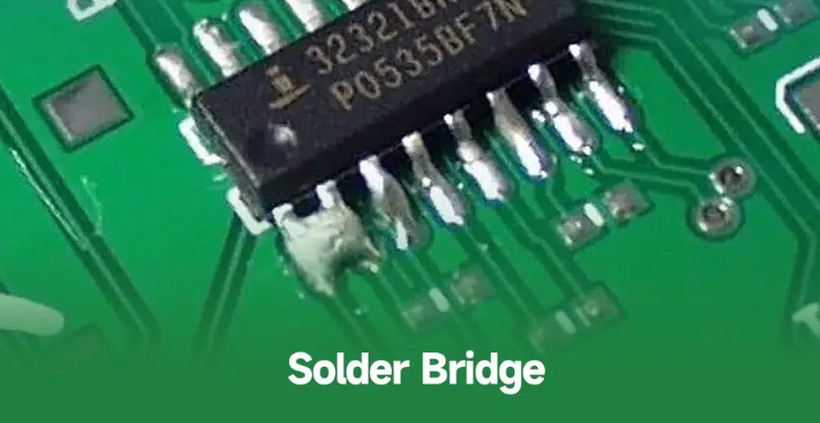
Solder bridging defects refer to unintended solder connections that form between two adjacent conductive elements, such as pins or pads, during the soldering process. These bridges create electrical shorts, which can lead to malfunctioning circuits, device failure, or even safety hazards in high-power systems.
These defects commonly occur in printed circuit board (PCB) assembly and semiconductor packaging, especially during reflow soldering, wave soldering, or hand soldering. Solder bridging is considered one of the most critical and frequent surface mount technology (SMT) defects.
Why Are Solder Bridging Defects a Serious Concern?
Solder bridging defects can cause:
- Short circuits: Direct electrical contact between unintended conductors.
- Intermittent failures: Solder bridges may break or form depending on thermal expansion.
- Component damage: Sensitive semiconductor components can be destroyed by shorts.
- Reduced yield: Bridging increases the rate of board rework or scrap.
- Quality control challenges: In high-density assemblies, inspection becomes more complex.
For industries relying on precision, such as aerospace, automotive, or medical electronics, the tolerance for such defects is extremely low.
What Are the Primary Causes of Solder Bridging Defects?
Understanding the root causes of solder bridging defects is key to prevention. The main contributing factors include:
a. Excessive Solder Paste
Too much solder paste applied during stencil printing can overflow between closely spaced pads, especially in fine-pitch components like QFPs or BGAs.
b. Inaccurate Component Placement
Misalignment during pick-and-place operations may cause solder to connect unintended pads.
c. Insufficient Solder Mask
Poor solder mask design or registration errors can reduce the insulation between adjacent pads, promoting bridging.
d. Improper Reflow Profiles
Incorrect temperature gradients or soak times during reflow soldering can affect solder wetting behavior and flux activation.
e. Poor Pad Design
Overly large pads or insufficient spacing between them create more opportunity for solder to flow into undesired areas.
f. Contamination
Residues such as dust, oil, or flux residue can alter the surface energy and solder flow, contributing to solder bridging defects.
How Do Solder Bridging Defects Impact Semiconductor Packaging?
In the context of semiconductor packaging, solder bridging defects become even more critical:
- Fine-pitch components in chip-scale packaging (CSP), ball grid arrays (BGA), and flip-chip configurations are more susceptible.
- Bridging in power semiconductor modules can lead to thermal runaway or catastrophic device failure.
- Void rates and hermetic sealing are also interconnected with solder bridging, especially in vacuum reflow or vacuum welding processes.
As component sizes shrink and interconnect density increases, the margin for error becomes minimal. This makes advanced process control and material consistency essential.
How Can Process Control Help Minimize Solder Bridging Defects?
Process control in electronics manufacturing is the most powerful tool to reduce solder bridging defects. It includes:
- Stencil design optimization: Using step-down stencils or nano-coatings to control paste volume.
- Solder paste inspection (SPI): Automated systems to check volume, height, and position before component placement.
- Placement accuracy: Regular calibration of pick-and-place machines to avoid shifts.
- Controlled reflow profiles: Monitoring zone temperatures, conveyor speed, and airflow.
- Statistical Process Control (SPC): Using historical data to anticipate deviations and implement corrections proactively.
What Role Does PCB Design Play in Solder Bridging Defects?
Design for manufacturability (DFM) plays a foundational role in solder bridging prevention:
- Proper pad spacing according to IPC guidelines reduces the likelihood of bridging.
- Solder mask dams between fine-pitch pads help isolate solder flows.
- Thermal relief patterns avoid heat imbalances that promote bridging.
- Via-in-pad structures should be designed carefully to prevent solder wicking into vias, which can cause uneven distribution.
Using DFM tools and collaborating early with the PCB fabricator can significantly reduce these risks.
Can Vacuum Soldering Effectively Prevent Solder Bridging Defects?
Vacuum soldering has gained traction in high-reliability electronics due to its ability to:
- Eliminate voids in solder joints by reducing entrapped gases.
- Improve solder wetting due to controlled pressure and heat profiles.
- Enhance flux efficiency, as vacuum conditions assist in vaporizing residues.
For power electronics and semiconductor packaging, vacuum reflow ovens are increasingly used. Companies like Chengliankaida Technology Co., Ltd. develop equipment specifically to address voids, hermetic sealing, and solder bridging defect prevention in semiconductor device packaging.
Vacuum soldering also enables lower defect rates in multi-layer modules or hybrid assemblies where traditional reflow processes fall short.
What Inspection and Testing Methods Help Detect Solder Bridging Defects?
To ensure solder bridging defects are caught early, manufacturers employ several methods:
- Automated Optical Inspection (AOI): Visual verification of bridges post-reflow.
- X-ray Inspection (AXI): Essential for hidden joints (e.g., BGA) or multilayer modules.
- In-Circuit Testing (ICT): Electrical continuity testing to detect shorts.
- Functional Testing (FCT): Confirms device operation under simulated real-world conditions.
- Microscopic Analysis: For process failure analysis and root cause identification.
Inspection is not only about detection—it’s also a feedback mechanism to fine-tune upstream processes.
How Is the Industry Innovating to Reduce Solder Bridging Defects?
Innovation to prevent solder bridging defects continues in multiple areas:
- 3D SPI & AOI Systems: More accurate analysis of paste and joints.
- Jet printing solder paste: Eliminates stencil limitations for small or irregular pads.
- Low-residue, high-reliability fluxes: Minimize bridging and cleaning steps.
- AI-driven process optimization: Algorithms that predict and correct potential defects.
- Integrated vacuum reflow ovens: Offering inline inspection and adaptive heating profiles.
Additionally, as chiplets and advanced packaging like 2.5D/3D ICs emerge, new standards are being developed to address solder bridging and similar interconnect challenges.
Conclusion: Toward Reliable and Defect-Free Electronics Assembly
Solder bridging defects are one of the most common and disruptive issues in modern electronics assembly. While they stem from various sources—design, materials, equipment, and process parameters—they can be effectively mitigated through a combination of:
- Careful PCB and stencil design
- Accurate solder paste application
- Precision in component placement
- Controlled reflow environments
- Adoption of vacuum soldering where applicable
- Comprehensive inspection strategies
By investing in process control and embracing innovation, manufacturers can significantly reduce solder bridging defects, ensuring higher product reliability, reduced rework costs, and improved customer satisfaction in today’s competitive electronics market.
Comments